Here we report on innovations and provide information that will help you: When it's about transport security and packaging, cocoon is the right contact.
Wenn sich vom 23. bis 25. Februar 2026 Experten aus Behörden und Streitkräften in Nürnberg versammeln, steht ein Thema im Fokus: Die Sicherheit Europas. Unter dem Leitsatz „Connecting Minds. Protecting Europe.“ bietet die Enforce Tac die Plattform für den fachlichen Austausch zu innerer und äußerer Sicherheit.
Wir bei cocoon verstehen diesen Auftrag wörtlich. Denn der Schutz von Menschenleben und kritischer Infrastruktur beginnt oft bei der Integrität der Ausrüstung. Ob hochsensible Optronik, komplexe Kommunikationssysteme oder taktische Bewaffnung – Einsatzbereitschaft setzt voraus, dass das Material unversehrt am Bestimmungsort ankommt.
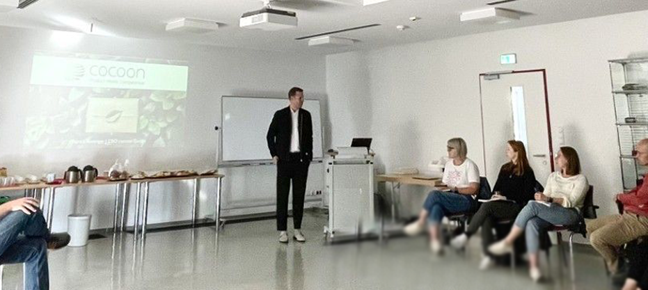
What does sustainable packaging mean in the photonics industry? What requirements apply to cleanrooms, international regulations and material responsibility? At the OptoNet e.V. ‘Sustainability’ working group, we discussed precisely this - together with representatives from industry, quality management and environmental responsibility. Our CEO Patrick Biesinger was there to provide imput with a presentation on current challenges and solutions relating to modern packaging systems - from legal labelling and material selection to recycling and reuse in the cleanroom environment.
Artikel anzeigenWhat does sustainable packaging mean in the photonics industry? What requirements apply to cleanrooms, international regulations and material responsibility? At the OptoNet e.V. ‘Sustainability’ working group, we discussed precisely this - together with representatives from industry, quality management and environmental responsibility. Our CEO Patrick Biesinger was there to provide imput with a presentation on current challenges and solutions relating to modern packaging systems - from legal labelling and material selection to recycling and reuse in the cleanroom environment.
Artikel anzeigenWhat does sustainable packaging mean in the photonics industry? What requirements apply to cleanrooms, international regulations and material responsibility? At the OptoNet e.V. ‘Sustainability’ working group, we discussed precisely this - together with representatives from industry, quality management and environmental responsibility. Our CEO Patrick Biesinger was there to provide imput with a presentation on current challenges and solutions relating to modern packaging systems - from legal labelling and material selection to recycling and reuse in the cleanroom environment.
Artikel anzeigenWhat does sustainable packaging mean in the photonics industry? What requirements apply to cleanrooms, international regulations and material responsibility? At the OptoNet e.V. ‘Sustainability’ working group, we discussed precisely this - together with representatives from industry, quality management and environmental responsibility. Our CEO Patrick Biesinger was there to provide imput with a presentation on current challenges and solutions relating to modern packaging systems - from legal labelling and material selection to recycling and reuse in the cleanroom environment.
Artikel anzeigenWhat does sustainable packaging mean in the photonics industry? What requirements apply to cleanrooms, international regulations and material responsibility? At the OptoNet e.V. ‘Sustainability’ working group, we discussed precisely this - together with representatives from industry, quality management and environmental responsibility. Our CEO Patrick Biesinger was there to provide imput with a presentation on current challenges and solutions relating to modern packaging systems - from legal labelling and material selection to recycling and reuse in the cleanroom environment.
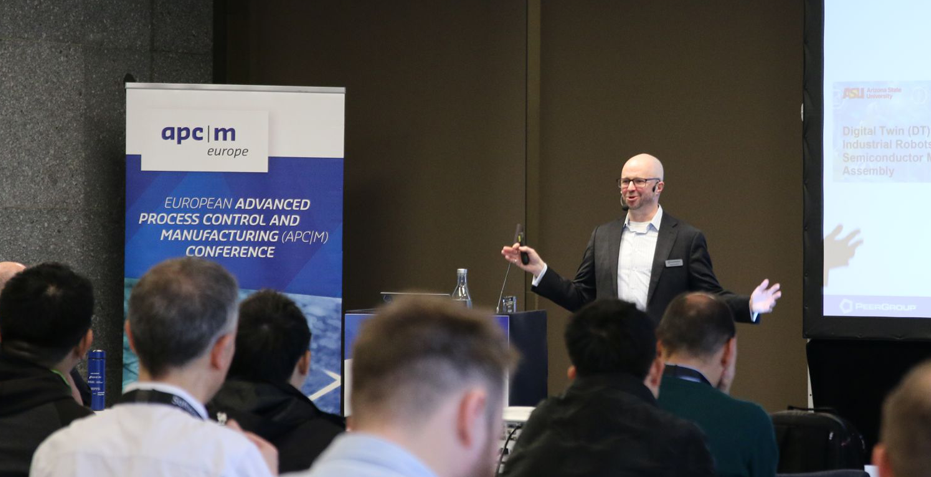
Artikel anzeigenAs part of the apc|m Europe Conference in Prague, cocoon GmbH was part of an international industry gathering focussing on advanced process control, smart manufacturing and sustainable technologies. Three days full of specialist presentations, innovations and personal dialogue showed how dynamically the semiconductor world is developing - and the role played by intelligent packaging solutions.
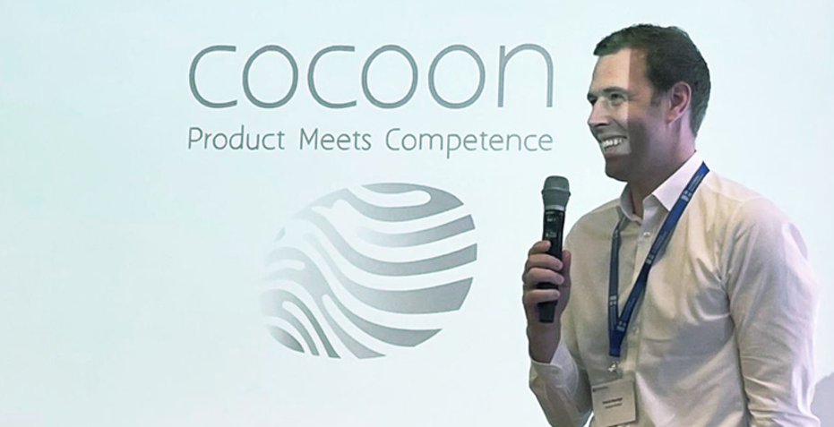
Artikel anzeigenIm Rahmen eines hochkarätigen Branchentreffens in der Schweiz war die cocoon GmbH – vertreten durch unseren CEO Patrick Biesinger – Teil eines intensiven Austauschs rund um Photonik, smarte Fertigung und Hightech-Innovationen. Mit dabei: führende Unternehmen, spannende Technologien und viele neue Impulse für unsere Verpackungslösungen von morgen.
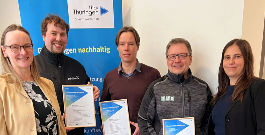
Artikel anzeigenNachhaltigkeit gehört für uns zum Selbstverständnis eines zukunftsfähigen Unternehmens. Um unser Engagement weiter zu vertiefen, haben wir mit anderen engagierten Thüringer Unternehmen an einer dreiteiligen Workshopreihe zur Entwicklung ganzheitlicher Nachhaltigkeitskonzepte teilgenommen: Im Mittelpunkt standen zentrale Handlungsfelder aus den Bereichen Ökonomie, Ökologie, Soziales und Management. Die gewonnenen Erkenntnisse fließen nun gezielt in unsere Arbeitsprozesse ein – und stärken unser Ziel, gemeinsam mit Kund:innen, Partnern und Mitarbeitenden an einer ressourcenschonenden, verantwortungsvollen und zukunftsfähigen Verpackungswelt zu arbeiten.
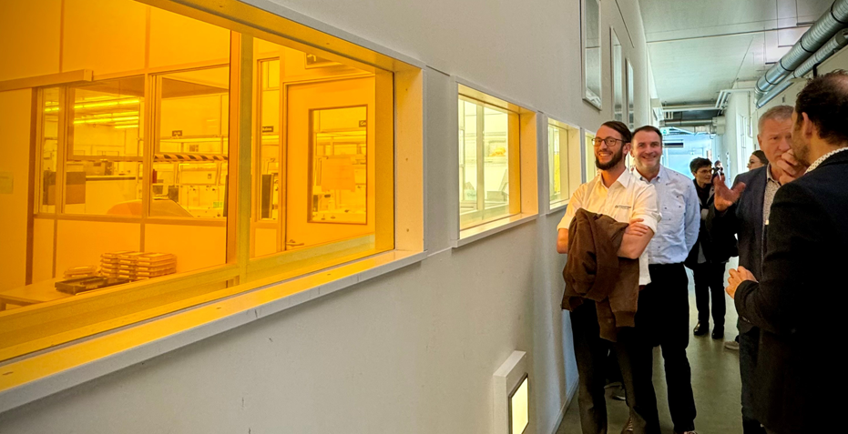
Artikel anzeigenUnser jüngster Besuch in den Niederlanden führte uns direkt ins Herz der europäischen Halbleiter- und Hightech-Branche – und war geprägt von spannenden Gesprächen, innovativen Ideen und inspirierenden Begegnungen. An Standorten wie dem High Tech Campus Eindhoven, dem Brainport Industries Campus, AMOLF, Holst Centre, SMART Photonics, der Technischen Universität Eindhoven, Demcon, Neways Electronics International NV, PhotonDelta, NTS, HighTechXL, dem Photonics Cluster Netherlands, Optics Netherlands und ASML durften wir erleben, wie vielfältig, zukunftsweisend und lösungsorientiert die technologische Landschaft unserer Nachbarn ist.
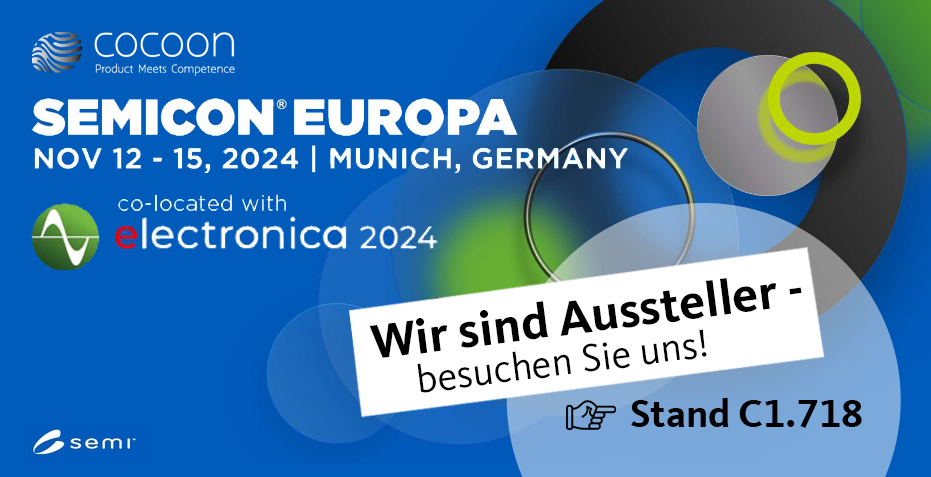
Artikel anzeigenWir freuen uns, in diesem Jahr als Aussteller auf der SEMICON Europa vertreten zu sein, einer der weltweit führenden Messen für die Halbleiter- und Mikroelektronikindustrie. Hier bieten wir unseren Kunden Einblicke in die neuesten Technologien und maßgeschneiderte Lösungen für ihre Anforderungen. Parallel dazu findet die electronica statt, die umfassende Innovationen entlang der gesamten Elektronik-Wertschöpfungskette präsentiert. Als Aussteller beraten wir Sie gern zu unseren reinraum-kompatiblen Verpackungslösungen und den Vorteilen für Produktschutz und Sicherheitsstandards. Besuchen Sie uns in Halle C1, Stand 718 – wir freuen uns auf Sie!
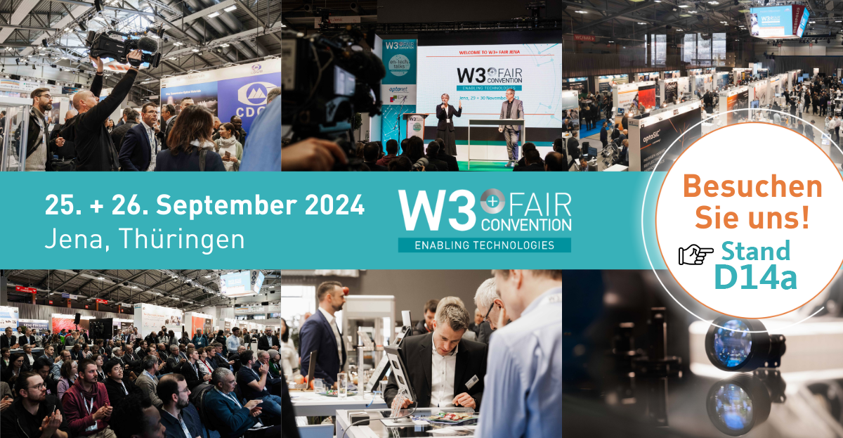
Artikel anzeigenW3+ Fair in Jena - die perfekte Gelegenheit, um zu erfahren, wie unsere Lösungen Ihr Geschäft verbessern können, Ideen auszutauschen und in interessante Gespräche über Verpackungslösungen und Produktschutz für Ihre empfindlichen Komponenten, Geräte und Großanlagen einzutauchen. Wenn Sie die W3+ Fair besuchen und ein Treffen oder ein kurzes Beratungsgespräch vereinbaren möchten, let’s make it happen - besuchen Sie uns an Stand D14a!
Artikel anzeigenInnovation means progress. The ZEISS Group has stood for quality in the optical and optoelectronic industry for 175 years. Continuous further development is essential. With 27 research and development locations worldwide, ZEISS invests in the future and generates unique ideas.
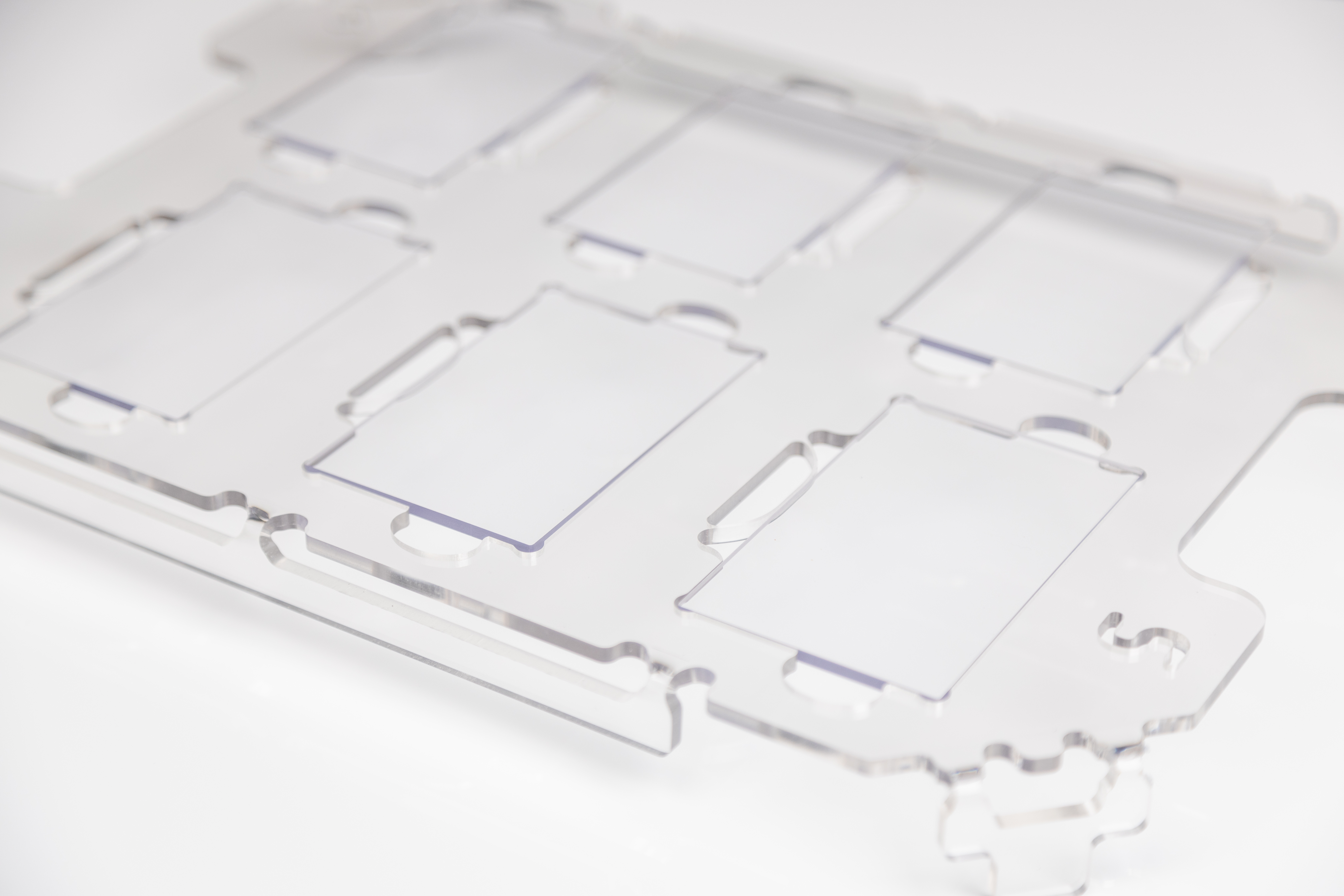
Show articleTransporting and storing optical components such as mirrors and lenses entails many challenges, as their surfaces are highly sensitive and thus cannot be used as contact points. We have developed a patented load carrier that uses the very narrow edges of technical mirrors and optical components as contact areas. The new solution is unique for its type and fills a significant gap in the market.
Show articleSectoral & market leaders entrust their high-quality products & important capital goods to out packaging from the start. This trust inspires our commitment. Our principle remains: considered customer benefit, at all times.